Are L and C Compatible? A Practical LC Circuit Design Guide
Explore whether inductors (L) and capacitors (C) are compatible in LC networks. Learn resonance, impedance, tolerances, layout tips, and best practices for reliable, tunable circuits.

Yes—L and C are compatible when used together in LC networks to achieve resonance and filtering. The key is understanding resonance, impedance, and parasitics. When values are chosen with target frequency and layout in mind, LC pairs enable precise tuning and stable operation, while poor matching or layout can cause instability.
Understanding the core question: are l and c compatible?
In electronics design discussions, the central question is often framed as: are l and c compatible within a given LC network? The short answer is that they can be used together to create useful resonant and filtering functions, but compatibility depends on context, frequency, and layout. L (inductors) store magnetic energy and grow their reactance with frequency, while C (capacitors) store electric energy and shrink their reactance as frequency rises. When you combine them, you get an LC network whose behavior depends on how you connect the two components and what else sits in the circuit. In practice, the question are l and c compatible is less about a binary yes/no and more about choosing the right values, tolerances, and parasitics for your target performance. In short, LC compatibility is achievable, but only with careful planning around resonance, impedance matching, and physical realization.
Key concepts you need: impedance, resonance, and Q-factor
Impedance is the sum of resistance and the reactive effects from L and C. For L and C, XL = 2πfL and XC = 1/(2πfC). When f changes, the balance shifts. Resonance occurs when XL equals XC, producing a peak or notch in impedance depending on the circuit topology. The resonant frequency is f0 = 1/(2π√(LC)). The quality factor (Q) describes how sharp the resonance is and depends on the inductor's series resistance, capacitor ESR, and other losses. Understanding these concepts helps answer the central question of compatibility because LC networks are most useful when you can predict how impedance changes with frequency and how sensitive the network is to tolerances.
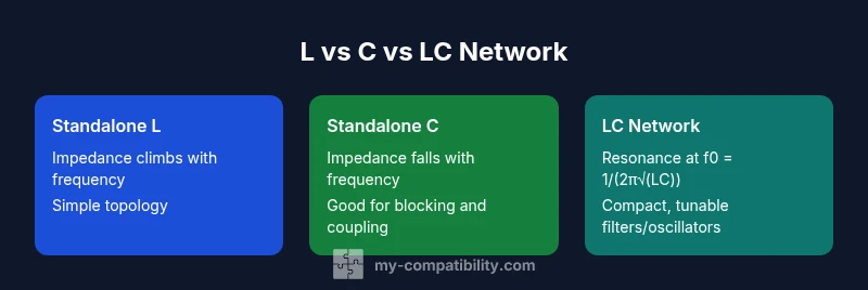
Standalone vs combined approaches
Standalone L-based designs emphasize inductive behavior for impedance shaping, while standalone C-based designs rely on capacitive effects for coupling and filtering. When used together as an LC network, you get tunable resonance, selective filtering, and the ability to shape bandpass or notch responses. The trade-off is added design complexity, tighter tolerances, and more attention to parasitics and layout. For some tasks, keeping L and C in separate stages reduces risk; for others, the compact LC network offers a clear performance edge.
Calculating resonant frequency and bandwidth
For a simple LC pair, f0 = 1/(2π√(LC)) defines the center frequency of resonance. Bandwidth depends on the overall Q and surrounding component losses. In practical designs, you must account for stray inductance and stray capacitance from traces and pads, which can shift f0 and broaden or narrow the response. A good practice is to compute an initial estimate using nominal L and C values, then tighten the design with simulation and measurement to capture parasitics.
Practical tolerances and parasitics
Real components differ from their nominal values. Tolerances in L and C propagate to shifts in f0 and impedance. Parasitics such as PCB trace inductance, pad capacitance, and package effects can significantly alter the LC network. Designers mitigate this by selecting components with tighter tolerances for critical paths, using short, well-routed traces, and validating the layout with parasitic-aware simulations. A robust LC design plans for these deviations rather than assuming ideal behavior.
Layout and routing considerations for LC networks
Physical layout matters as much as the schematic. Keep LC paths short and direct, minimize loop areas, and separate high-current or high-frequency sections from sensitive nodes. Use ground planes to reduce EMI and avoid creating unintended coupled inductors or stray capacitances. Shielding and proper decoupling help maintain stability in powered LC networks. Finally, document clear reference planes and consistent grounding to ensure reproducible results across boards and vendors.
Choosing L and C values: rules of thumb
Start with your target f0 and a desired impedance level, then pick L and C to satisfy f0 = 1/(2π√(LC)) while achieving practical component sizes and tolerances. If space or cost is a concern, you can trade off by selecting a higher Q with quality components, which narrows the bandwidth and improves selectivity. For broadband requirements, consider a wider separation of L and C values to reduce sensitivity to parasitics, or use multiple LC sections to approximate a broader response.
Common pitfalls and how to avoid them
Avoid placing LC networks near high-current paths, which can introduce parasitic inductance and magnetics. Do not neglect parasitics in the PCB stackup; include them in your simulations. Be wary of core saturation in inductors at high power, and verify capacitor voltage ratings match peak operating conditions. Finally, always validate with measurement and adjust values to compensate for real-world behavior rather than relying solely on nominal calculations.
Real-world examples: filters, oscillators, and tuning
LC networks shine in RF filters, where sharp selectivity is essential, and in oscillators, where a resonant tank defines frequency. In audio and control systems, LC elements can be used for tunable filters and impedance matching networks, enabling compact designs. Real-world success depends on careful selection of component quality, layout discipline, and precise testing across the intended operating range.
Testing and verification: measuring L-C compatibility
Verification begins with an LCR meter to check component values, followed by network analysis to observe the actual impedance vs frequency. Use a vector network analyzer for precise measurements of S-parameters and to confirm resonance characteristics. Build a test fixture that minimizes extraneous parasitics and repeat tests across multiple boards or batches to ensure reproducibility.
Safety, reliability, and manufacturing considerations
Inductors may saturate, capacitors may exhibit voltage-dependent behavior, and both parts can drift with temperature. Factor these effects into derating and environmental specifications. In production, ensure you have robust selection criteria, traceable components, and consistent assembly processes to maintain LC consistency across lots. Reliability planning helps prevent drift that could shift resonance outside the desired band.
Design checklist for LC compatibility
Create a written checklist: target f0 and impedance, select L and C values with tolerance margins, model parasitics, verify PCB layout, confirm voltage and current ratings, simulate across temperature, and plan test procedures. This structured approach reduces rework and yields predictable LC performance.
Final considerations: future trends in LC design
As manufacturing tolerances tighten and simulation tools improve, LC designs become more accurate and repeatable. Advanced materials and compact, high-Q inductors reduce size without sacrificing performance. Designers increasingly rely on parasitic-aware optimization, multi-section LC networks, and automated verification to maintain compatibility across evolving product families.
Feature Comparison
| Feature | Standalone L-based designs | Standalone C-based designs | LC network (L and C together) |
|---|---|---|---|
| Impedance behavior | Inductive impedance increases with frequency | Capacitive impedance decreases with frequency | XL and XC interact to form a frequency-dependent impedance |
| Resonant potential | No inherent resonance on its own | No inherent resonance on its own | Resonance at f0 = 1/(2π√(LC)) that can be tuned |
| Complexity | Simpler, fewer components; easier layout | Simple path for coupling and DC blocking | Higher design complexity due to parasitics and layout |
| Best use case | RF inductive networks, chokes, impedance shaping | Coupling, DC blocking, and RC-like filtering | Tunable filters, oscillators, and compact resonant tanks |
Positives
- Enables precise impedance shaping with minimal parts
- LC networks offer compact, tunable filters and oscillators
- High-Q performance with quality components
- Good for targeted RF and high-frequency applications
Cons
- Higher design complexity and tighter tolerances
- Pronounced sensitivity to parasitics and layout
- Potentially higher cost and board area for discrete LC tanks
LC networks provide versatile performance when designed with parasitics in mind
If your goal is precise tuning and compact filters, LC offers advantages. If simplicity and cost are primary, separate L or C stages may be preferable.
Questions & Answers
Are LC components interchangeable if I want to swap L for C to achieve the same resonance?
No. Replacing L with C changes the resonance condition and the impedance profile. A swap alters the fundamental relationship and the filter or oscillator behavior. If you need a different resonance, recalculate f0 and re-validate the circuit with simulations and measurements.
Swapping L and C changes resonance; you must recalculate and re-test.
How do parasitics affect LC networks on a real PCB?
Parasitics from traces, pads, and nearby components can shift resonance and broaden or distort the response. Include parasitics in your model, use short, direct routing, and consider shielding to minimize these effects.
Parasitics matter. Model them and keep layouts tight.
What is the best way to calculate the resonant frequency of an LC pair?
Use f0 = 1/(2π√(LC)) for a single LC tank. Validate with circuit simulation and measurement to account for real-world parasitics and tolerances.
Compute f0 with the LC formula and verify with tests.
Are there safety concerns when using inductors at high power?
Yes. Inductors can saturate under high power, causing nonlinear behavior. Ensure components have adequate current ratings, proper derating, and thermal management.
Yes—watch for saturation and heat.
How can I quickly check LC compatibility during prototyping?
Use an LCR meter to verify values, then perform a network-analysis sweep to observe resonance and impedance across the target band. Adjust L or C as needed.
Measure values and sweep the network to verify resonance.
What is a quick rule of thumb for selecting L and C values?
Choose L and C to target the desired f0 first, then adjust to meet impedance and size constraints while tolerating component variation.
Target f0 first, then adjust for size and tolerance.
Highlights
- Define target frequency before selecting L and C
- Model and mitigate parasitics from the start
- Use LC for tunable filters and oscillators
- Layout matters: keep traces short and well-placed
- Validate with simulation and real-world testing